Using voltage glitching to unleash the A100 in my mining card
On this page
Summary
I’ve discovered a voltage fault injection vulnerability on the GA100 die, allowing an operator to blow arbitrary fuses. Utilizing this vulnerability, I’ve converted my CMP 170HX 8GB card into what is effectively an A100-80G! Further, my unlocked cards actually perform ~1.2x faster than a retail A100 by having all functional SMs enabled (~120-126, die-lottery dependent), rather than the yield-safe 108 SMs NVIDIA chose for all production A100 cards. Finally, CMP-disabled features like NVLink, PCIe Gen4, NVJPG, NVDEC, MIG are all unlockable with this approach, though I haven’t specifically tested NVJPG/NVDEC/MIG.
Here’s how my “A100-80G” appears and functions.
00000000:81:00.00x20C210DE00000000:C1:00.00x20C210DEFull nvidia-smi output
$ nvidia-smi --query-gpu=index,pci.bus_id,pci.device_id,name,memory.total; nvidia-smi topo -m
index, pci.bus_id, pci.device_id, name, memory.total [MiB]
0, 00000000:81:00.0, 0x20C210DE, NVIDIA Graphics Device, 81920 MiB
1, 00000000:C1:00.0, 0x20C210DE, NVIDIA Graphics Device, 81920 MiB
	GPU0	GPU1	CPU Affinity	NUMA Affinity	GPU NUMA ID
GPU0	 X 	NV12	0-127	0		N/A
GPU1 NV12 X 0-127 0 N/AFull OpenCL output
.-----------------------------------------------------------------------------.
|----------------.------------------------------------------------------------|
| Device ID    0 | NVIDIA Graphics Device                                     |
| Device ID    1 | NVIDIA Graphics Device                                     |
|----------------'------------------------------------------------------------|
|----------------.------------------------------------------------------------|
| Device ID      | 0                                                          |
| Device Name    | NVIDIA Graphics Device                                     |
| Device Vendor  | NVIDIA Corporation                                         |
| Device Driver  | 610.43.03 (Linux)                                          |
| OpenCL Version | OpenCL C 3.0                                               |
| Compute Units  | 124 at 1410 MHz (7936 cores, 22.380 TFLOPs/s)              |
| Memory, Cache  | 81338 MB VRAM, 3472 KB global / 48 KB local                |
| Buffer Limits  | 20334 MB global, 64 KB constant                            |
| Max Workgroup  | 1024 threads                                               |
|----------------'------------------------------------------------------------|
| Info: OpenCL C code successfully compiled.                                  |
| FP64   Compute   (double, fma  )                     11.287 TFLOPs/s (1/2 ) |
| FP32   Compute   (float , fma  )                     22.781 TFLOPs/s ( 1x ) |
| FP16   Compute   (half2 , fma  )                     85.858 TFLOPs/s ( 4x ) |
| INT64  Compute   (long  , a*b+c)                      2.759  TIOPs/s (1/8 ) |
| INT32  Compute   (int   , a*b+c)                     22.769  TIOPs/s ( 1x ) |
| INT16  Compute   (short2, a*b+c)                     20.273  TIOPs/s ( 1x ) |
| INT8   Compute   (char4 , dp4a )                     81.169  TIOPs/s ( 4x ) |
| Memory Bandwidth ( coalesced read      )                       1883.17 GB/s |
| Memory Bandwidth ( coalesced      write)                       2137.93 GB/s |
| Memory Bandwidth (misaligned read      )                       1460.81 GB/s |
| Memory Bandwidth (misaligned      write)                        250.13 GB/s |
| PCIe   Bandwidth (send                 )                         13.10 GB/s |
| PCIe   Bandwidth (   receive           )                         11.69 GB/s |
| PCIe   Bandwidth (        bidirectional)            (Gen3 x16)   11.58 GB/s |
|-----------------------------------------------------------------------------|
'-----------------------------------------------------------------------------'
NVIDIA uses fuses for product segmentation, security features, and other fun access control features - and crucially, there are several functions where blowing a fuse on an NVIDIA die can grant you more access, not less. In a properly secured design, a blown fuse should always induce a more restrictive state, because a blown fuse cannot be unblown in an economically feasible way. NVIDIA’s design allows one to relax restrictions by blowing more fuses!
In this post, I will go over the GA100 die, its fuse controller, the use of VFI, and future research directions. I’ve decided to publish some of the work that enabled my research here.
Acknowledgements
My work builds on prior research by Jon Pry and numerous others who have dedicated much of their time towards better understanding the GA100 die. I am disclosing my findings subsequent to another security researcher independently discovering the same vulnerability; I believe it to be in the best interest of the public to make this information publicly available. These findings were disclosed to NVIDIA’s product security team ahead of the publication of this article.
GA100 versions
The GA100 is an NVIDIA die that has been used to power almost 20 different SKUs - the A100 being the most well-known variant. I won’t delve into every SKU, but I will present the GA100 manifestations that matter to my work, covering the different versions of the CMP 170HX and the A100.
As fabbed, the GA100 die has 128 SMs, 12 FBPs, 5 NVDEC units, a PCIe Gen4 x16 controller, and depending on the framebuffer size, comes with 4-6 stacks of HBM co-packaged with the die. NVIDIA uses eFuses for yield-control and product segmentation–undifferentiated GA100s turn into more restrictive variants based on defect testing and manufacturer demand.
In one of the most extreme manifestations of product segmentation, the CMP 170HX, an Ethereum mining card with nominally 8 or 10 GB of application-exposed framebuffer capacity, actually comes with, respectively, ~80 and ~40 GB of HBM onboard! This work chiefly centers around how to fully unlock and use that capacity. Previous work has made great strides in unlocking the GA100 via software methods; VFI takes us across the last mile.
| SKU | Out-of-box | Software (cmpunlocker) | GA100VFI |
|---|---|---|---|
| CMP 170HX 8GB | |||
| Framebuffer | 8 GB | 64 GB | 64-80 GB1 |
| CMP 170HX 10GB | |||
| Framebuffer | 10 GB | 40 GB2 | 40-48 GB |
| Both CMPs | |||
| SMs | 70 | 70 | 120-128 |
| PCIe generation | 1 | 2 | 4 |
| NVLink | No | No | Yes3 |
| ECC | No | No | Yes4 |
| Multi-Instance GPUs | No | No | Yes4 |
| NVDEC | 0 | 0 | 54 |
Hardware restrictions
So, how does NVIDIA utilize fuses to produce both a datacenter A100 and a mining CMP card from one die? To understand this, we need to take a closer look at the fuse controller located on the GA100.
The fuse controller is a block that contains 16,384 eFuses (512 rows of 32) and a bunch of logic surrounding that raw fuse macro. Its job is to perform fuse readout and programming, protect the underlying fuses, and provide usable “option words” to the rest of the die. These option words subsequently decide how the die functions and what features are enabled.
Each eFuse can be in one of two states (blown=1, unblown=0), and the 512 rows are divided into 4 regions:
- Regular fuses (rows 0-221). These are straightforward; often single (pairs of) fuses will map to an option word, such as OPT_ENABLE_FUSE_PROGRAM (an option word that determines whether further fuse programming is allowed or not). Regular fuses have built-in redundancy: for example, OPT_ENABLE_FUSE_PROGRAM consists of a PRI and RED (primary and redundant) fuse, in this case the primary instance is fuse 0 of row 0, and the redundant is fuse 0 of row 1. Some option words are scalars, such as OPT_X_COORDINATE, which is 9 bits wide and ostensibly holds the x-coordinate of the die on the fabbed wafer. Importantly, if a regular fuse is blown, there is basically no remedy to persistently unblow it (save for RIR later).
- Fuseless fuses (rows 222-487). This is a weird one. Apparently NVIDIA got frustrated with accidentally blowing regular fuses and ruining their engineering samples, and came up with a system to encode effective option words in a JTAG chain-like format (see this patent). Think about FF as essentially a script that describes what option words should have what values. FF fuses (excuse the RAS syndrome) concern most of the functionality we can unlock using VFI. This is because FF option words can be trivially cleared by simply writing new FF rows! We’ll about this more in depth, later. For now, you should know that NVIDIA also knows this, because under normal conditions, you are strictly prevented from performing any FF fuse blows.
- IFF fuses (rows 487-512). These contain instructions in a different format than the FF one. They’re out of scope for this post, and they’re mainly useful for on-the-fly reprogramming of fuse controller option words. They are usually not accessible in a production card.
- RIR fuses (8 rows of 32 fuses, which are technically not part of the 512 rows). These are provided by the designer of the fuse macro (TSMC datasheet here) and are essentially the first party designer’s intended “fuse repair” mechanism. The RIR section on a GA100 has space for 16 repair instructions, each overriding the value of an identified single fuse in the main 512 rows. Unfortunately for us, specifically in the 8 GB 170HX SKU, 15 of the 16 RIR words are all ones, and the 16th word encodes a useless repair instruction that can only be rarely leveraged for any interesting unlock. The story is different for the 10 GB SKU, but that’s a matter for another day…
There are two really interesting groups of fuses for the VFI-based unlock:
- “Control fuses”. The term comes from NVIDIA’s Tegra hardware headers, they use it to refer specifically to rows 0 and 1, which specify the values of highly security-sensitive option words.
- Fuseless fuses, which encode all of the interesting option words that decide whether a GA100 is born to be a measly mining card or an AI datacenter workhorse.
Before we name some of the FF-encoded option words, we’ll have to first understand the FF record format in a bit more detail, then talk about the die blocks that govern the features we are interested in.
Fuseless fuses
Each FF row is a 32-bit record. Bits 0–4 select a chain, bit 5 distinguishes FF from IFF (0 for FF), bits 6–15 select a 16-bit block, and bits 16–31 supply that block’s new value. The JTAG-chain picture from the patent is quite literal here: the controller builds the option data by replaying these records into chains. Fixed locations in each chain correspond to individual option words.
If two records address the same chain and block, the later record wins. For example, 0x0fe805c1 means chain 1, block 23, data 0x0fe8. Appending that record can clear an effective bit set by an earlier FF record. No physical fuse is unblown; a new row replaces the old 16-bit block. This works for FF-backed options, not the regular control fuses in rows 0 and 1.
Now that we know how FF words are encoded, here’s a list of the interesting words and their locations. These were discovered by a particularly helpful researcher who cross-compared FF values and effective option words from different GA100 SKUs in order to differentially understand the FF chain/block to option word mappings, as there is no known official mapping.
| Named option | Inferred FF location | Use |
|---|---|---|
NV_FUSE_OPT_FBIO_DISABLE |
Chain 1 bits 83–106; blocks 5–6 | Memory I/O floorsweep |
NV_FUSE_OPT_FBPA_DISABLE |
Chain 1 bits 107–130; blocks 6–8 | Memory subpartition floorsweep |
NV_FUSE_OPT_GPC_DISABLE |
Chain 1 bits 131–138; block 8 | GPC floorsweep |
NV_FUSE_OPT_TPC_GPC0_DISABLE through NV_FUSE_OPT_TPC_GPC7_DISABLE |
Chain 1 bits 187+8i through 194+8i for GPC i; blocks 11–15 |
Eight TPC masks |
NV_FUSE_OPT_PES_DISABLE |
Chain 1 bits 251–274; blocks 15–17 | PES floorsweep |
NV_FUSE_OPT_FBP_DISABLE |
Chain 1 bits 307–318; block 19 | Framebuffer partition floorsweep |
NV_FUSE_OPT_ROP_L2_DISABLE |
Chain 1 bits 319–342; blocks 19–21 | ROP/L2 floorsweep |
NV_FUSE_OPT_NVLINK_DISABLE |
Chain 1 bits 368–370; block 23 | NVLink disable mask |
NV_FUSE_OPT_DISABLE_GEN3_SPEED |
Chain 2 block 39; which of bits 1 and 9 is unresolved | PCIe Gen3 speed restriction |
NV_FUSE_OPT_PCIE_MAGIC_BITS_D[25] |
Chain 2 block 47 bit 3 | Gen4 speed-disable flag |
NV_FUSE_OPT_PCIE_BOOT_GEN23_DISABLE |
Chain 2 block 49 bit 6 | PCIe boot policy |
NV_FUSE_OPT_PCIE_BOOT_GEN3_DISABLE |
Chain 2 block 49 bit 7 | PCIe boot policy |
NV_FUSE_OPT_PCIE_DEVIDA |
Chain 2, bits 593–608; blocks 37–38 | Device identity |
NV_FUSE_OPT_PCIE_DEVIDB |
Chain 2, bits 609–624; blocks 38–39 | Device identity |
NV_FUSE_OPT_SYS_PIPE_DISABLE |
Chain 1, bits 372–379; block 23 | Multi-instance GPU enabled pipes |
The acronyms FBIO/FBPA/FBP/TPC/GPC/PES/ROP all refer to microarchitectural elements, please see this diagram from the GA100 whitepaper to further understand how these are related to each other:
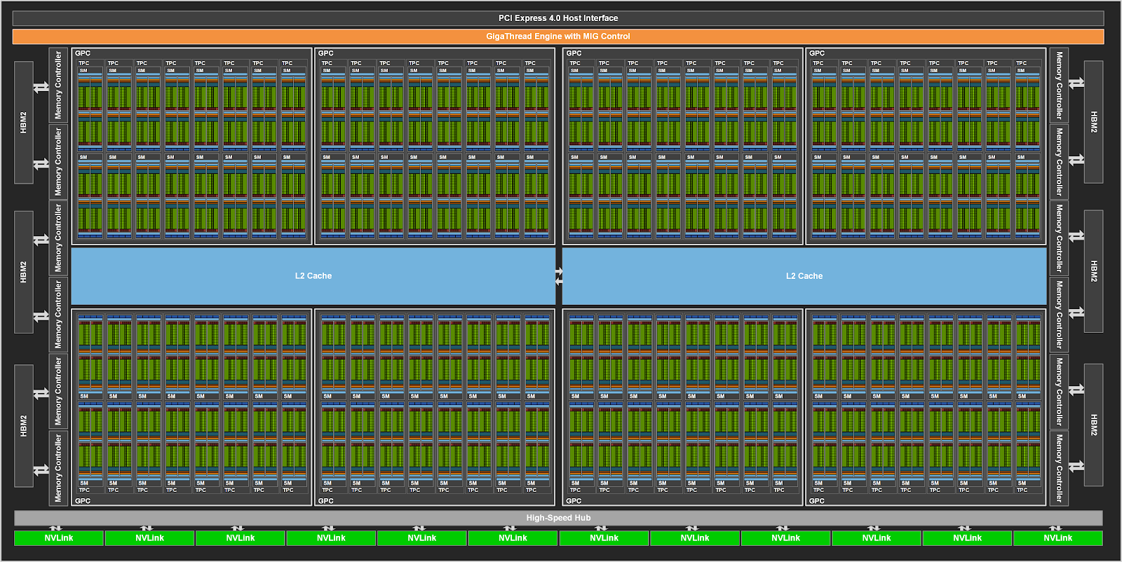
FBP is the internal NVIDIA term for a “framebuffer partition”, with 2 FBPs to one HBM stack. FBPAs are subpartitions, 2 FBPAs to one FBP. PES/ROP are blocks (seemingly graphics-related) that are required for an SM to function.
With this knowledge in hand, what if we could write new FF rows that set the _DISABLE words to be all zeroes, or at least, as permissive as possible given die defects? If we look at how the _DISABLE options are used in conjunction with other elements, we’ll quickly see that these _DISABLE words are the primary lever we have in preventing parts of the die from being “floorswept”. After illuminating the “what-if”, I’ll talk about the “how”: the exact application of voltage fault injection and the fuse controller safeguards we can defeat with VFI.
Floorsweeping
NVIDIA puts these options in charge of setting floorsweep signals, which will render a die element unreachable (and likely powered down). From experiments, I believe the floorsweep lines are specified in RTL, emanating from the fuse controller and terminating in individual functional blocks and controlling some master power/clock domain switch within the block. I have observed the floorsweeping behavior to correspond with very little latency with the value of the fuse controller’s effective status words for each functional block.
Let’s take FBP floorsweeping, for example. On one of my 8 GB cards, OPT_FBP_DISABLE was 0x852: FBPs 1, 4, 6, and 11 were masked. The separate OPT_FBP_DEFECTIVE mask was 0x840, covering 6 and 11. After I reduced the FF-backed disable mask to 0x840 with a replacement FF row, the extra masks on 1 and 4 were gone, but the defective 6 and 11 stayed disabled. That leaves 10 of the die’s 12 FBPs in the effective mask. Functionally, FBPs 1 and 4, which refused register reads and writes when OPT_FBP_DISABLE was 0x852, became responsive after this fuse write.
Although the functional blocks can be “unfloorswept” with FF writes, this does not fully suffice to render the block fully available to an end application - the default framebuffer geometry configuration uses only a portion of each available HBM stack, for example.
To bypass that, we can utilize what is essentially a small modification to cmpunlocker’s method. The usual driver patch for the 8 -> 64 GB unlocks writes to a particular set of feature configuration words (FBPA_CFG, SM_SPEED_SELECT, etc.). The default values are chosen to succeed for the commonly found variant of the 170HX, which has the _DISABLE FF-derived option words preventing certain functional blocks from being used (any attempt to use them will return floorswept errors). With the unlocking FF burns in place, we can write even more permissive words into the configuration registers, resulting in what is functionally an A100-80G.
Achieving the FF burn
With the information we have, it seems straightforward that if one could blow arbitrary FF fuses, any GA100 could be fully unlocked to its maximum capability, as determined by die yield and the populated memory stacks. But how do we blow FF fuses? Let’s take a look at the fuse programming functionality of the fuse controller to understand more.
To request a fuse blow, one must write to the FUSEADDR, FUSEWDATA, and FUSECTRL registers belonging to the fuse controller. Although not nominally accessible to the host or to unprivileged requesters, with the Canary in the Crypto Mine ROP, opening up the responsible privilege level masks is trivial. And so, many researchers have attempted to coerce the fuse controller to blow fuses in the FF region. Some of our shared observations follow:
- The fuse controller has an internal FSM, and it indicates its current state via the FUSECTRL_STATE bits.
- The fuse controller enters a WRITE_PROGRAM state per each “hot” bit in the requested FUSEWDATA value. This tracks with the expected fuse programming behavior.
- However, unless a specific option word is cleared, writes to fuse addresses outside of the FPF range (rows 96-221) do not actually take place. Fuses in this region (believed to be “field programmable fuses” indicating a watermark of which ucode versions have run, alongside other field-relevant information) do take effect, and the fuse controller state machine behaves identically between FPF and non-FPF regions.
The specific option word I am referring to is OPT_SECURED_BURN_FEATURE_ENABLE (“SBFE”), and it is set to be 1 in all production cards. When this option word is clear, fuse programming is allowed in any address. When it is set, only FPF fuses may be blown. To date, no one has found any way to burn FF fuses with SBFE=1, even when operating the fuse controller from HS contexts. It is not clear what “secured burn” truly means, I speculate that there must be a software-only way to perform non-FPF burns even with SBFE=1, and we just don’t know what the “secured” adjective really means here.
Note PLM, HS, ucode, …; I am delving into using a bunch of NVIDIA-specific terminology in this section as the explanation gets deeper. For a really in-depth explanation of what these mean, I refer you to other sources such as Je Ne Sais Quoi - Falcons over the Horizon.
Importantly, as people have figured out on more permissive cards, it is possible to perform FF burns with SBFE=0! And as it turns out, achieving this state is how we achieve the GA100 unlock. After much trial-and-error, I have resorted to inducing this state via voltage fault injection, and I was able to achieve it. Let’s talk some more about voltage glitching.
Voltage fault injection
Much has been said about VFI, and I’ll leave the in-depth explanation to other sources. In short, applying brief pulses of low supply voltage will often cause unexpected behavior in integrated circuits. I asked GPT-6 Astra to design an STM32G4 based board that taps into the PWMVID signal on the CMP PCB. PWMVID is an NVIDIA standard for voltage regulators, and my glitcher intercepts the PWM signal emitted by the GA100 die, and replaces it with its own waveform fed into the MP2888B VRM driver IC. With my setup, I can induce the card’s own VRM to produce timed glitches for me, which is simpler than MOSFET-based setups and enables faster glitching than attempting to directly drive the PMBus.
The glitcher requires two connections to the PCB, ideally done with magnet/enameled wire. One wire taps NVVDD for voltage sensing, and another wire taps the PWMVID signal. The only other required step for the glitcher to function is the removal of a 0402 0ohm resistor, which will break the connection between the GA100 output PWM pin and the VRM IC. Finding where to place the taps is trivial by tracing the pinout of the MP2888B, specifically its PWMVID and VOSEN pins (the MP2888B shares a footprint with its sibling public chip MP2888A). Test points directly adjacent to the MP2888B enable relatively easy installation of the PWMVID tap.
With this tap in place, a single glitch attempt involves this sequence:
- Remove card power
- Apply card power
- Start a timer (“glitch timer”) as soon as NVVDD crosses a threshold
- Execute a proposed voltage waveform by issuing a PWMVID signal, aligned to the glitch timer
- Observe card behavior, repeat from step 1 as needed
My setup achieves steps 1/2 with a simple ACPI S0 -> S3 -> S0 transition, which can be done in a few seconds on a modern desktop platform. More intrusive modifications or expensive rigs can probably achieve a better experiment rate, but in my experience this setup suffices to unlock cards in somewhere between 1 hour and 48 hours of glitching time using the approach described later.
For the NVVDD threshold, the Astra-authored firmware uses an STM32 comparator to detect when NVVDD crosses 225mV, after which a tight DMA loop drives the desired duties on the PWMVID pin. After S0, the host inspects the card state and decides what to do next; if it involves another glitch, the glitcher board will be commanded over USB with a glitch pattern. Then the host induces S3 with an RTC timer to wake back up in ~3s (empirically derived period for decent stability).
Sometimes the host will fail to return to S0, I’ve remedied this with relegating bookkeeping and glitch campaign preparation to an SBC (Radxa Cubie A5E) which also can drive the motherboard power/reset button pins via GPIO if the glitch target host is unresponsive.
More specifics are shared in the GA100VFI repository if you’re interested. For now, let’s take a look at the different interesting states we can trigger via VFI, as well as the specific glitch state that we need to burn FF rows. To help illuminate the differences between each glitch state, I have built an empirical model of how the fuse controller starts up when voltage is applied. Note that without the RTL that implements the fuse controller, all we have are guesses. Here are the hypothesized boot stages:
- Sense RIR, as required by the fuse macro
- Sense (from fuse macro into readout register) control rows
- Latch control rows into control row-derived option words
- Sense remaining rows
- Latch regular fuse values into their option words
- Parse FF chain
- Latch FF chain values into their option words
These hypothetical stages are based on what I can actually read from the die: controller states, raw rows when CMD_READ works, the published option words, and whether the PRI ring can still reach the rest of the GPU. By looking at a few key values, we can tell glitch outcomes apart. Importantly, glitch patterns and outcomes are very much die-specific, so consider these example waveforms and responses to be just that, examples. Let’s take a look at 3 interesting glitch states.
1. All fuses sensed as zero
Some glitches make almost every published option word read as zero. In one captured state, 669 of 672 named option reads were zero; the other three were error responses. The controller’s CRC status was 0x00 (not parsed yet), the PCIe ID read as 2080 (the base GA100 PCIe product ID, does not correspond to a real retail product), and the GPU’s PRI ring was held in reset.
This state is consistent with a catastrophic failure on behalf of the fuse controller. The card comes up basically unusable, because almost all boot functions are disrupted by the all-zero state. However, interesting enough, the card trains at PCIe Gen4 natively! Some slightly altered variants may showcase sections of fuses being successfully latched, or containing garbled values instead of all-zeroes. I was not able to push any of these states towards an FF burn; in almost all of them the fuse controller is unreachable or dysfunctional.
2. RIR read disrupted
Reading the RIR data on the CMP 170HX 8GB reveals its exact effect: 15 noop repair instructions, and one write that changes the value of a fuse in row 18, whose option word we can monitor. Further, because the RIR sense is consumed internally by the fuse macro instead of directly by the fuse controller, we can observe a disrupted RIR latch by attempting to read the raw row - the observed bitflip remains consistent across the flipped option word as well as the raw fuse row. This sets an interesting chronological checkpoint in investigating die boot (RIR sense must happen prior to other fuse sensing), but is not a useful glitch in itself.
3. Goldilock’s glitch
The successful three-pulse state on my first card seemed to disrupt precisely the row0/1 based option words, while leaving other fuses and option words intact. In this state, all of the row0/1 derived option words are zero. The initial readbacks look like this:
| Signal | Initial readback |
|---|---|
| PCI ID and access | 20c2; BAR0 and the PRI ring respond |
FUSECTRL |
0xe0040000 (IDLE) |
CRC_ |
0x55 (both halves parsed without errors) |
DISABLE_ |
0 |
OPT_ |
0 |
ENABLE_ |
0 |
| FUSECTRL/FUSEOPT privilege masks | 0xffffffff for both |
| Raw rows 0 and 1 | Both still 0x53557c3d, unchanged from before the glitch |
At this stage, we are still not yet capable of issuing FF writes, because ENABLE_FUSE_PROGRAM=0. I am honestly not sure why ENABLE_FUSE_PROGRAM would ever be zero, given it’s 1 in retail boards, so this almost reads to me like a way to implement a glitch-detection canary (or at least it would be elegant to do so).
Fuse sensing happens one row at a time, with all 32 fuses powered for sensing with one line, meaning it is much more challenging for an attacker to make a single fuse appear as cleared or set. It would make sense, then, to include a “canary” fuse that disables security-critical features (like fuse burning) when it is cleared, because usually the attacker can only manipulate fuse sensing at the row granularity at most. So, when the row0/1 option words come up as all cleared, ENABLE_FUSE_PROGRAM=0 stops us from burning any fuses.
However, take a look at what we have in this state: DISABLE_SW_OVERRIDE=0. This word is normally 1, and it stops us from setting the EN_SW_OVERRIDE register to 1, which then lets us “shadow” most of the option words exposed by the fuse controller. Doing so involves writing to a register CTRL_OPT_*, corresponding to option word OPT_*, which then determines the effective value STATUS_OPT_*. This is what lets us shadow SBFE to be 0. But, even though we have DSOV=0, ENABLE_FUSE_PROGRAM turns out to be one of the option words that are impossible to shadow, even with DSOV=0. So it seems we’re stuck.
At least that’s what I thought, and I banged my head against the wall in this state for a while. Then I noticed that there is one fuse controller command I haven’t tried issuing yet: SENSE_CTRL. I had refrained from issuing this, because on the face of it it seems like all of the row0/1 (control fuse) derived option words would match their fused values, which would reset SBFE, turn off software option word shadowing, and leave us unable to fuse. To my surprise, when I issued this command, all of the control-fuse-derived options went to their fused value, except DISABLE_SW_OVERRIDE, which remained 0!
With DSOV=0, we can trivially set SBFE to 0, ENABLE_FUSE_PROGRAM is 1 because it matches its fused value, and we are off to the races! One wrinkle remains in that FUSEWDATA may have a locked down PLM, but with DSOV=0, we can just write 0 to OPT_SECURE_FUSE_WDATA_WR_SECURE to set the PLM to be all-ones, opening host access for fusing.
At this point, all that’s left to do is to calculate _DISABLE words that match the _DEFECTIVE values for the features we are interested in, and issue FF burns. Note that the occupied FF space and defective bits differ per die, so each burn must be die-tailored.
End results
Framebuffer unlock
On 8 GB cards with 80 GB intact (seems to be around ~90% of 8 GB cards from my limited sample size), the unlock yields the full 80 GB as a usable framebuffer. Multiple synthetic tests (writing pseudorandom words throughout the full framebuffer and reading them back after L2 invalidation) as well as real workloads (such as vLLM and SGLand) are fully functional. As mentioned, one of my cards has only 64 GB intact. In this case, the hardware unlock yields no framebuffer advantage.
Compute unlock
The 170HX is limited to 70 SMs out of the box. In practice, there are almost always >120 SMs non-defective on the die, and the unlock allows using them all. This results in a significant performance uplift, ~1.7x compared to the software-only 170HX unlock, and even an impressive ~1.2x over a retail A100!
PCIe generation
The only thing that stops cmpunlocker from advancing beyond PCIe Gen2 are the FF option words. With relevant bits cleared, Gen3/4 train and are confirmed to be fully functional. When combined with the PCIe decoupling capacitor mod, up to PCIe Gen4 x16 is attainable, matching a retail A100 PCIe variant.
NVLink
Zeroing out the OPT_NVLINK_DISABLE word is only one of the required mods for NVLink to actually work. Because the CMP 170HX PCB is missing the U11 IC (which connects PCIe 3.3v to an NVLink bridge pin), a stock board fails to bring up the reference clock generator on attached NVLink bridges. Simply bridging two of the pins on the footprint of U11 resolves this issue, although it removes whatever regulation or protection was provided by U11. Be careful if you’re bridging GPUs powered by different power supplies, as this will connect the +3.3V rails together unless you leave U11 unpopulated on some of your GPUs! The NVLink bridge works fine if you just patch U11 on one of the boards in the pair.
On the firmware side of NVLink enablement, there is a ROM check that needs to be bypassed with additional host-side commands. I’m sure your clanker can figure it out ;)
While investigating the NVLink unlock, I also found a few interesting quirks with NVIDIA’s NVLink implementation on the GA100. I will be posting a further blog post on this, so stay tuned!
Future directions
With arbitrary fuse burning, we mostly gain feature unlocks. Some security-sensitive options are shipped unblown by default, and burning them may lead to interesting footholds. But what’s more interesting to me are the deeper glitch states where many default-blown security-sensitive fuses sense unblown, enabling routes like debug HS execution, which grant unprecedented access to die internals.
References
- Jon Pry, A Canary in the Crypto Mine: Defeating Stack Protection in a GPU Secure Coprocessor (2026).
- Amogh Munikote, cmpunlocker (2026).
- Otto Bittner et al., The Forgotten Threat of Voltage Glitching: A Case Study on Nvidia Tegra X2 SoCs (2021).
- NVIDIA, US9230678B2: Integrated circuit having an enhanced fuseless fuse structure (2016).
- TSMC, TEF07F32X32HD18_PHRM_C180518 electrical fuse datasheet, rev. 120A (2018).
- hexkyz and SciresM, Je Ne Sais Quoi - Falcons over the Horizon (2021).
- TechPowerUp, NVIDIA GA100 GPU specifications.
- GA100VFI source repository.
Footnotes
-
Anecdotally, out of the 10 specimens of CMP 170HX 8 GB I have examined, only one has shipped with only 64 GB usable, the rest all have a functional framebuffer size of 80 GB. ↩
-
Although the Canary in the Crypto Mine paper claims a stable 80 GB on the 10 GB SKU, very few, if any, cards in the wild have been able to achieve this, and solid evidence is scarce. It remains plausible that some number of 10 GB SKUs really do come shipped with 80 GB on-board, however the percentage seems very low according to the community. Most “unstable” 80 GB unlocks are explained with a combination of L2 caching and memory aliasing over a true 40 GB framebuffer. ↩
-
Enabling NVLink further requires a very small hardware mod due to a missing component on the 170HX PCB, I’ll talk more about this later. ↩